Big Blue has developed technology it hopes will support semiconductor developments for the next decade
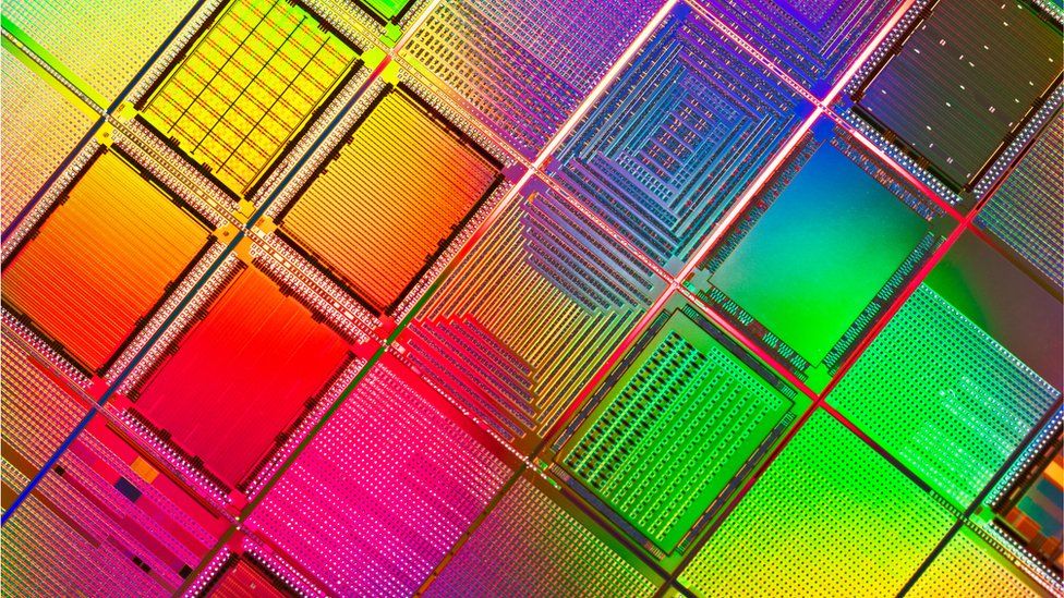
IBM has unveiled what it claims is a breakthrough in semiconductor technology. Working with industry partners, the company sees no wall in semiconductor development that cannot be chipped away.
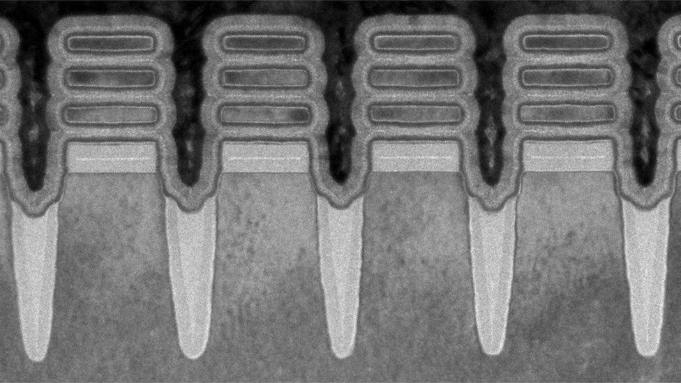
As more things get connected, there is increased demand for chip performance and energy efficiency. IBM said its newly developed 2 nanometer (nm) nanosheet technology helps advance the state-of-the-art in the semiconductor industry, addressing this growing demand. According to IBM, chips developed using 2 nm technology could achieve 45% higher performance, or made to run 75% more energy efficiently when compared with today’s most advanced 7 nm chips.

IBM vice-president of hybrid cloud research Mukesh Khare described the breakthrough as a facet of IBM’s research, which aims to drive semiconductor scaling to support the hardware required for hybrid cloud computing in the datacentre.
Researchers estimate that datacentres consume 1% of global electricity usage. According to IBM, changing all datacentre servers to 2 nm-based processors could potentially reduce that number significantly.
Khare described the 2 nm technology as “foundational logic”, which would meet the density, power and performance requirements for logic and memory chips, in both low-power and high-performance applications.
In conjunction with public and private sector industry partners, Khare said the semiconductor research at IBM’s semiconductor research centre in Albany, New York has the potential to drive chip technology for the next decade.
IBM works with a number of semiconductor partners to package and produce the chips it designs.

In March, IBM forged a partnership with Intel to drive semiconductor innovation. Such partnerships are seen as key to driving future developments in semiconductor technologies.
At the time, Dario Gil, director of IBM Research, said: “No single company, no matter how significant, can create and bring to bear the power of many of these technologies alone. IBM is a proponent of partnerships to accelerate innovation in the industry and has cultivated a thriving semiconductor research ecosystem in Albany, NY.”
He said the company has partnered with Samsung Electronics in the manufacture of the IBM 7 nm chips, the first of which will come to market later this year in IBM Power 10-based systems. Gil said the collaboration with Intel would accelerate the velocity of packaging and process innovations into the future.
When asked if the semiconductor industry faces a wall, which will stop future breakthroughs, Khare said: “With the partnership we have and that amount of talent and energy, there’ s not a wall we can’t break through.”
Application areas for the technology range from chips with 50 billion transistors to a handheld mobile device, with an estimated battery life of four days, IBM said.
Production of semiconductors based on the 2 nm technology is expected to start in 2024.
Vocabulary
- quadruple: Increase or be increased by four times
- breakthrough : A sudden, dramatic, and important discovery or development
- measure: Find the size, amount, or degree of something
- artificial: Made by people rather than occurring naturally, especially as a copy of something natural.
- Incredibly: Extremely or unusually.
Comprehension
What does the article say tablets and smartphones can do these days?
How much data does the article say we can store on our smartphones?
How much less energy do the new chips use?
What could the new chips do to mobile phone battery life?
How often might we be charging our mobile phones?
What is the size of IBM's new chip?


