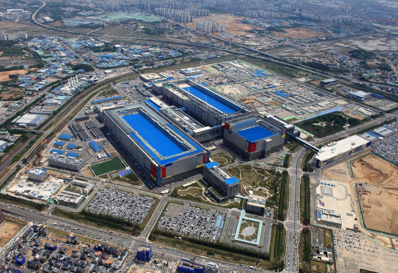
 Samsung's Pyeongtaek chip plant (Samsung Electronics)
Samsung Electronics is anticipated to finalize its investment plan for foundry expansion in the United States and South Korea, and make it official as early as next month, according to industry forecasts on Monday.
After participating in the meetings with US President Joe Biden and Korean President Moon Jae-in last week, Samsung seems to be accelerating its internal decision-making process to finalize the investment plan both for Korea and the US in response to the two governments’ calls.
The total investment amount for at least two new fabs – one likely in Austin, Texas, and the other in Pyeongtaek, Gyeonggi Province is estimated to be over 50 trillion won ($44.7 billion). Some forecast the figure could reach 70 trillion won.
It has been revealed through filings by Texas authorities that the Korean chipmaker is planning to build a $17 billion foundry fab in Austin. Samsung has also talked with other US states including Arizona and New York, but Austin seems to be the most viable option, considering its current operations and ample tax incentives.
A recent Texas power outage triggered by a winter storm, which caused the Samsung plant in Austin to freeze its operation for more than a month, has given Samsung an edge in its negotiations with Texan authorities to win greater benefits from them.
It is highly likely that Samsung could announce the US investment before President Moon’s planned visit next month to the US for a summit with President Biden.
Samsung remains silent on the company’s schedule for the upcoming investments.
In Korea, Samsung has been laying the groundwork for its third fab in Pyeongtaek, to be called “P3,” which will be the most cutting-edge foundry fab in the country.
The company was expected to come up with the P3 investment plan in the second half of this year, but industry observers believe the plan could be moved forward considering the talks with President Moon and the government’s upcoming policy package for the chip industry.
The P3 fab is being planned to be built on land with an area of 700,000 square meters, which is expected to be the world’s single largest. It would be 1.75 times larger than Samsung’s second fab, in which it injected 30 trillion won.
Samsung also plans to equip the new fab with the most advanced extreme ultraviolet lithography equipment, which costs nearly 200 billion won per unit.
Industry observers predict that the P3 investment could be as big as 40 trillion to 50 trillion won.
With regard to Samsung’s hesitant stance on its investment plans, leaders of the Korean business community have made requests to the government to pardon Samsung’s chief Lee Jae-yong.
On Friday, Sohn Kyung-shik, chairman of the Korea Enterprises Federation, suggested granting a pardon for the imprisoned Samsung chief to Hong Nam-ki, the country’s top economic policymaker, during a meeting with government officials.
“In the US, the president is taking the lead in reviving its semiconductor industry,” Sohn said. “Frankly, I am worried that Korea, the world’s chip powerhouse, could lose its position in the market.”
Words in this Article
Foundary – n. a factory where metal is melted and poured into specially shaped containers to produce objects such as wheels and bars
Accelerate – v. to happen or make something happen sooner or faster
Filling – n. the activity of putting documents, electronic information into files
Ample – adj. more than enough
Fab – n. a factory for making advanced electronics products, for example silicon ships
Comprehension Quiz
What is this article mainly about?
According to industry forecasts, what is anticipated by Samsung Electronics?
Where are the two new fabs for the investment?
Why was the power outage occurred in Texas and what happened to the Samsung plant due to Texas power outage?
What does the word, “P3” refer to?


